New large-scale instrument for research in the nanometer range
School, ZEITlab |

The dual-beam FIB (Focused Ion Beam) is the new centerpiece of the ZEITlab, the technology hub of the TUM School of Computation, Information and Technology. The ZEITlab combines neuro- and bioengineering, chemistry, nanostructuring, microelectronics, measurement technology, assembly and connection technology as well as prototyping in a joint laboratory network.
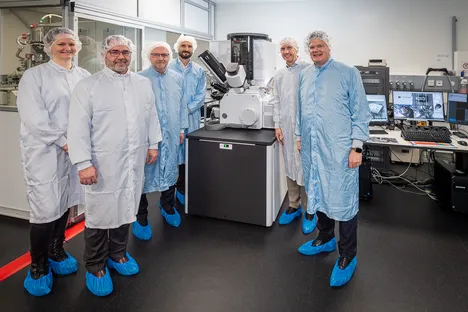
The large-scale instrument was procured by the technology group Rohde & Schwarz as part of a sponsorship agreement on permanent loan to the Technical University of Munich (TUM) and now enables science and industry to carry out precise material processing in the nanometer range. The dual-beam FIB is ideal for developing prototypes in particular.
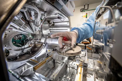
The highly sensitive instrument is located in the southwest section of the ZEITlab clean room in the new building for electrical engineering and information technology, which is due to open in 2022. Inconspicuous to the untrained eye, it can be seen from the visitor corridor through a window next to an atomic force microscope and a new electron beam lithography system. Working with it requires protective clothing and clean room gloves in order to ensure that the analyzed samples and the instrument itself are not exposed to contamination.
Dual-beam FIB: a microscope for high-precision work
A dual-beam FIB is a microscope that uses two beams simultaneously:
- An electron beam (SEM – Scanning Electron Microscope), which is used for high-resolution imaging of samples
- An ion beam (FIB – Focused Ion Beam), which is used to selectively ablate, cut or process materials.
With a dual-beam FIB you can therefore:
- Ablate material with high precision (for example, prepare semiconductor samples, expose structures, visualize defects)
- Produce thin sections for transmission electron microscopy (TEM) analysis largely automatically
- Selectively deposit metals and insulators, create or modify nanostructures
- Repair faults in semiconductor circuits on-chip (editing circuits)
- Change properties of thin films in a targeted manner, produce prototype metamaterials
- Analyze the topography of nanostructures using a variety of detectors and evaluate material and crystal contrast qualitatively and quantitatively
- Enable 3D imaging through step-by-step ablation (3D tomography)
In short, the dual-beam FIB combines high-resolution imaging with precise material processing and material analysis on the micro- and nanometer scale. It is the “Swiss army knife” of nanotechnology.
"A haven of joy and innovation"

Together with Alexander Braun, Vice President for Digitalization and IT Systems at TUM, Hans-Joachim Bungartz, Dean of the CIT, and representatives of the professorial staff of the Department of Electrical Engineering, a delegation from the technology group Rohde & Schwarz came to view the measuring instrument on 30 January 2025.
Christian Leicher, Managing Director and Chief Executive Officer of Rohde & Schwarz, described TUM as a “haven of joy and innovation”. He himself studied Electrical Engineering and Information Technology at TUM and is still very attached to his alma mater. He sees it as a “beacon of confidence” and was therefore happy to accept the invitation to TUM. As part of the sponsorship agreement, the ZEITlab is also open to Rohde & Schwarz employees for failure analysis, chip modification and material analysis.
FIB technology has a long tradition at the CIT
FIB technology has been used at TUM since 1999. The first FIB instrument at an engineering faculty in Germany was installed at the then Chair of Technical Electronics. In close cooperation between industry and science, the technology has developed rapidly over the last 25 years.
Since then, this technology has been used for routine tasks such as circuit editing and cross-section analysis and is now an essential method for direct structuring and implantation tasks in research. For example, “optical elements” for so-called spin waves (lenses, gratings, zone plates, etc.) can be prototypically produced in thin yttrium iron garnet films (YIG for short) using precisely adjusted ion irradiation. This method was recently published in the journal Small by a team of TUM researchers and is expected to result in significantly scaled high-frequency components for on-chip applications.
